
Email Id: sale@adctooling.com
Choosing the right Fpga Chip can shape a product’s speed, power use, and long-term reliability. A device that looks affordable on a comparison table may demand costly thermal design later. Engineers often begin with logic cells, yet that is only one part of the decision. Memory blocks, DSP slices, transceivers, I/O standards, and package options can change the entire design. The board tells the truth. A crowded prototype board, a warm voltage regulator, or a delayed signal can expose assumptions early.
This guide presents ten practical tips for evaluating an Fpga Chip across real project conditions. It considers workload size, clock targets, development tools, supply stability, security features, and expected production volume. It also examines documentation quality and vendor support, because a strong specification cannot repair unclear timing guidance. In lab work, teams sometimes select generous logic capacity but overlook available memory bandwidth. That was expensive. A careful comparison should include power estimates at idle, typical operation, and peak utilization. Thermal limits should be checked with the intended enclosure, not an open bench.
No selection method is perfect. Early requirements change, prices move, and promising tools may feel difficult after several weeks. Therefore, each tip connects datasheet evidence with measurable tests, such as compiling a representative design and monitoring resource margins. Independent benchmarks can help, but they require careful interpretation. Readers should question vendor claims, record assumptions, and keep a second device under review when supply risk matters. The strongest choice is rarely the largest Fpga Chip. It is the device that fits performance, power, skills, budget, and future constraints without hiding uncomfortable trade-offs.
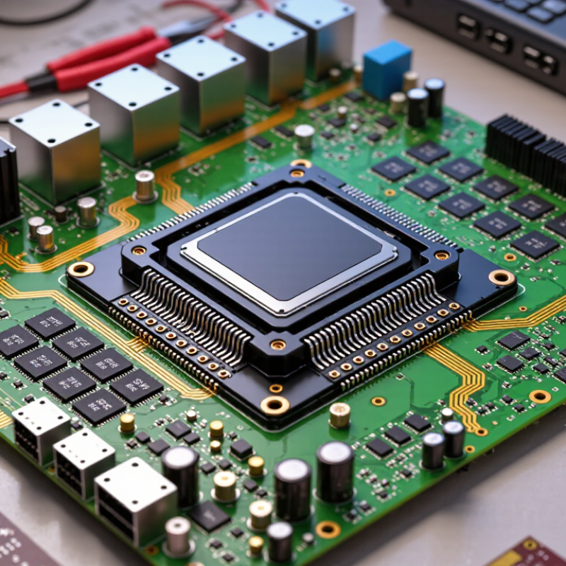
10 Tips for Choosing the Right FPGA Chip?
Define the FPGA Application, Performance Goals, and System Requirements
Choosing the right FPGA chip starts before comparing logic cells or package sizes. Define the application in operational terms: sensor fusion, motor control, video processing, or a custom data path. Then describe the system’s real workload. What enters the device? How quickly must it respond? Does it run continuously or in bursts? A clear use case prevents attractive but unsuitable specifications from driving the decision. It also exposes constraints such as board area, heat dissipation, power rails, and field-update needs. Small details matter.
Tip 1: Set measurable performance goals. Translate “fast” into clock rates, latency, throughput, and timing margins. For example, a design may need 2 GB/s sustained throughput with less than 10 microseconds of latency. Include worst-case traffic, not only laboratory averages. Leave room for future design changes. I have seen projects fail because resource estimates ignored debugging logic and interface overhead. That mistake is common. Recheck it.
Tip 2: Match resources to the architecture. Estimate lookup tables, registers, memory blocks, arithmetic units, transceivers, and I/O standards. Compare these needs with thermal limits and available power. A chip with abundant logic may still be wrong if its memory ports or package pins do not fit the board. Tip 3: Validate the system early. Build a small prototype with representative data, then review timing, utilization, power, and tool reports. Ask an independent engineer to challenge the assumptions. Requirements often change after testing. Plan for that reality.
| Tip | Selection Dimension | Application Definition | Performance Goals | System Requirements to Verify | Practical Selection Guidance |
|---|---|---|---|---|---|
| 1 | Define the primary workload | Classify the design as signal processing, industrial control, networking, image processing, data acquisition, or hardware acceleration. | Identify the dominant operation, such as filtering, packet handling, motor control, video pipelines, or custom parallel computation. |
| Choose an FPGA architecture whose embedded resources match the workload instead of selecting mainly by logic-cell count. |
| 2 | Estimate logic and register capacity | Determine the size of the intended RTL design, including control logic, datapaths, state machines, and interface logic. | Plan for implementation utilization below 100%; a practical design target commonly leaves approximately 10–20% capacity for timing fixes and future changes. |
| Use post-synthesis and post-place-and-route estimates where possible, because RTL size alone does not predict final resource usage accurately. |
| 3 | Match DSP and arithmetic resources | Identify multiply-accumulate operations, finite impulse response filters, transforms, matrix calculations, and fixed-point datapaths. | Calculate operations per sample, samples per second, operand width, and required parallelism. |
| Select sufficient dedicated DSP blocks to avoid implementing large multipliers only with general-purpose logic. |
| 4 | Size on-chip memory correctly | Account for buffering, line stores, coefficient tables, packet queues, frame storage, and processor firmware. | Determine total bytes, number of simultaneous buffers, read/write ports, access latency, and required memory bandwidth. |
| Check both memory capacity and port configuration; adequate total memory may still fail if the required parallel access pattern is unavailable. |
| 5 | Set clock frequency and latency targets | Define whether the system requires deterministic low latency, high throughput, or both. | Specify clock frequency, cycles per transaction, end-to-end latency, initiation interval, and data throughput. |
| Evaluate timing using realistic constraints and placement conditions; a higher nominal speed grade does not guarantee timing closure for every design. |
| 6 | Verify I/O and protocol compatibility | List all connections to sensors, converters, processors, storage devices, displays, and communication equipment. | Define interface data rates, lane counts, transaction sizes, and allowable latency or backpressure. |
| Confirm that the package provides enough correctly positioned pins and that the I/O banks support the required voltage and signaling standards. |
| 7 | Check processing-system requirements | Decide whether the design needs only programmable logic or also requires embedded processors for configuration, control, networking, or software tasks. | Estimate processor workload, interrupt rate, firmware memory, operating-system needs, and hardware–software communication bandwidth. |
| Use a device with an integrated processing subsystem when it reduces board components and meets the software workload without excessive external hardware. |
| 8 | Evaluate power and thermal limits | Define the operating environment, duty cycle, enclosure size, cooling method, and maximum allowable temperature. | Estimate static and dynamic power at the intended voltage, clock frequency, toggle rate, memory activity, and transceiver usage. |
| Perform power estimation early and include startup, worst-case workload, configuration, and transceiver power in the thermal analysis. |
| 9 | Plan configuration and security | Determine how the FPGA will load its design in production, during field updates, and after power interruptions. | Specify configuration time, update frequency, recovery behavior, and protection requirements for the bitstream and stored data. |
| Choose configuration features that support reliable boot, secure updates, rollback or recovery, and protection of application intellectual property. |
| 10 | Confirm package, lifecycle, and development support | Assess PCB constraints, production quantity, qualification requirements, maintenance period, and development-team experience. | Compare achievable performance after place-and-route with the available tools, reference designs, verification flow, and schedule. |
| Make the final choice only after confirming that the device can be sourced, designed in, tested, supported, and maintained for the full product life. |